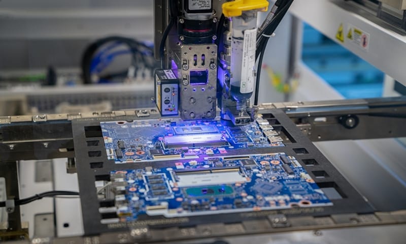
OMRON’s Inspection System Business Division participated in SEMICON Taiwan 2024. In this article, we introduce the latest product, VT-X950, which utilizes our proprietary CT-X-ray imaging technology to rapidly inspect the solder joint condition of the packaging structure of semiconductors. The VT-X950 employs high-speed imaging technology and automated inspection techniques, derived from X-ray inspection in the SMT substrate domain, where it holds a top global market share, now applied to semiconductor advanced packaging inspections.
For customers in the semiconductor industry worldwide, from research and development to mass production, we are committed to improving development speed, enhancing yield, and stabilizing mass production quality by providing tailored solutions to meet each customer’s specific needs at every stage of semiconductor manufacturing.


